Advanced Plasma Etching Solutions
Optimize plasma etching with Semion RFEA, Quantum RFEA, and Octiv VI probes for superior etch selectivity, surface quality, and profile precision
An etching window refers to the specific range of plasma process parameters (such as time, pressure, gas flow rates, power, and temperature, ion flux and ion energy) within which the etching process can effectively and precisely remove material from a substrate. Achieving the desired etching characteristics while maintaining the integrity and functionality of the remaining material depends on careful control of the etching window. Below are discussed the crucial factors affecting etching windows.
Ion energy
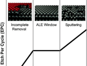
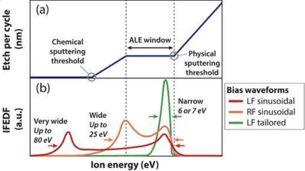
To control etch depth per cycle, self-limited surface reactions are needed, minimizing both spontaneous chemical etching and physical sputtering. The ALE window, shown in Figure 1, lies between incomplete etching and physical sputtering regimes. It indicates that a minimum ion energy is required to start etching, with the rate increasing linearly as ion energy rises, but exceeding a certain threshold leads to over-etching or surface damage. Effective etching requires maintaining ion energies within these thresholds, keeping ion energies typically at 100 eV or lower to minimize sputtering and surface damage, necessitating precise control of ion energy and distribution width.
DC Bias Voltage
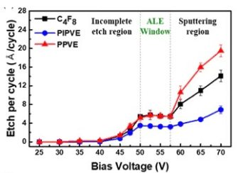
The DC bias voltage plays a crucial role in regulating the ion energies involved in the etching process. As illustrated in Figure 2, a linear etch rate is observed in relation to substrate bias during the etching window. Ion energy directly increases with bias voltage, allowing for precise control over the etching process.
Tailored Waveform Biasing
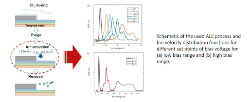
Anisotropic etching requires directional ions with specific energy to selectively remove materials. Precise energy control, independent of ion flux, is achieved using low-frequency (few kHz) tailored waveform bias applied to the wafer. These waveforms create narrow ion energy distribution functions, enabling accurate selection of etching windows, as shown in Figure 3.
Neutral to ion flux ratio
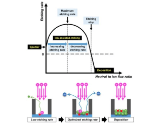
When the target material is exposed to simultaneous energetic ion and radical fluxes, understanding the impact of radical flux is crucial, as these radicals supply chemical reactants to the surface. As shown in Figure 4, the total etch rate with both neutrals and ions is higher than with either alone. The two extreme regimes, sputtering and deposition, show negligible etching rates due to a lack of chemical reactants and excessive deposition, respectively. Thus, measuring the neutral-to-ion ratio is essential for effective process control.
Impedans solutions to identify etching window
The Semion RFEA system has been useful in improving etch selectivity as it provides precise and accurate measurements of ion energy and flux. Octiv VI probe provide additional control on the process to improve the etch selectivity by measuring the various DC and RF parameters such as bias voltage, voltage waveform, duty ratio, etc of the plasma and biased electrode. These measurements provide direct inputs to modify the ion energies and hence the selectivity of the process.
One primary goal in developing etching processes is achieving atomic-scale selectivity between different materials, as shown in Figure 6. Advanced semiconductor devices often require simultaneous etching control over multiple materials, and the factors influencing etch selectivity are discussed below.


Figure 6 Schematic illustration of etch selectivity. (a) Before etch (b) after etch (c) bad selectivity and (d) good selectivity
Ion Energy Control for Etch Selectivity
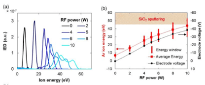
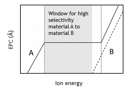
To optimize etching selectivity, it’s important to operate close to the energy threshold for physical sputtering of one material while taking advantage of the differing threshold energies among various materials (see Figure 7). For instance, the threshold energy for SiO2 is higher than that for Si, represented as Epsth(SiO2) > Epsth(Si). Consequently, controlling ion energy is crucial for enhancing selectivity, making accurate measurement of ion energy essential.
Substrate Bias to Improve Selectivity
A novel approach gaining traction is using surface bias to enhance etching selectivity. By adjusting the surface bias voltage, power, and pulse duty ratio, a range of ion energies can be generated for selective etching of different materials.
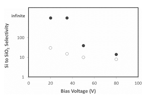
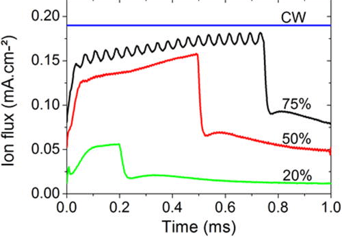
Figure 8 compares selectivity between silicon and silicon oxide for Atomic Layer Etching (ALE) and continuous processing with a Cl2/Ar gas mixture. For ALE, silicon oxide shows no significant etch rate at RF bias voltages up to 40 V, indicating an “infinite selectivity” region. In contrast, continuous processing shows a decline in selectivity at bias voltages above 0 V, highlighting the effectiveness of substrate bias in optimizing etching selectivity.
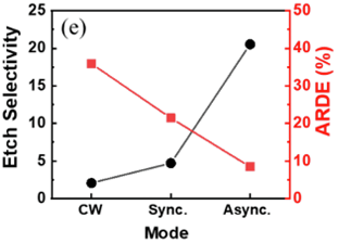
Also, etch selectivity increases in both synchronous and asynchronous biasing modes as compared to CW RF bias application as illustrated in figure 9. Therefore, precise and accurate measurement of bias voltages/pulse features becomes important to improve the selectivity.
Impedans solutions to improve etch selectivity
The Semion RFEA system has been useful in improving etch selectivity as it provides precise and accurate measurements of ion energy and flux. Octiv VI probe provide additional control on the process to improve the etch selectivity by measuring the various DC and RF parameters such as bias voltage, voltage waveform, duty ratio, etc of the plasma and biased electrode. These measurements provide direct inputs to modify the ion energies and hence the selectivity of the process.
Surface roughness is undesirable because it introduces variability and defects that degrade device performance. Plasma, used as an ion source for etching, can produce a wide ion energy distribution (IED), causing problems. If ion energy exceeds the ALE window, it can surpass the material’s binding energy, increasing surface roughness. Conversely, if ion energy is too low, it may not effectively remove the modified layer, resulting in poor surface morphology.
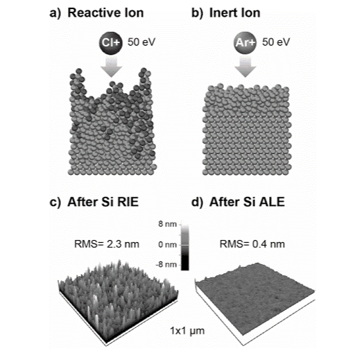
Achieving atomically smooth surfaces requires regulating the energy distribution width to match etching process requirements. Atomic Layer Etching (ALE) produces smoother surfaces than Reactive Ion Etching (RIE), as shown in Figure 11, indicating that surface roughness is related to the radical-to-ion flux ratio. Thus, monitoring both ion energy and the ion-to-neutral ratio is essential for optimizing surface roughness.
Impedans solutions to improve surface roughness
Direct measurement of ion energy and ion flux using the Semion RFEA system will be useful in improving the surface roughness. Also, adequate adjustment of RF biasing and plasma power using Octiv VI probe will be helpful to achieve smoother surfaces.
In semiconductor manufacturing, achieving precise etch profiles is crucial for device performance and yield. However, several challenges often arise during the etching process as shown in figures 13, 14 and 15.

Figure 13 Inside view of plasma process and typical challenges occurred to control the etch profile.

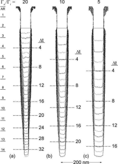
Figure 14 Showing the various deformation generated in etching profile due to uneven ion bombardment during the etching process. 3D view of bowing and twisting in HAR etching is shown in right image.

14 B transport limitation can lead to distortion(bowing and twisting) CD variation and incomplete etch during chanel formation.

Figure 15. Loading effect observed in batch processing.
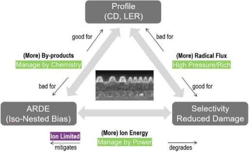
Impedans Limited offers cutting-edge sensor solutions to address the above said challenges, enhancing profile control during the etching process. Our suite of RFEAs, Langmuir probes and VI sensors provide precise measurements and insights, enabling superior etch profile management. They help to provide insights which help engineers and researchers to balance the complex tradeoffs (see figure 16) to create consistent reliable processes.
The Semion RFEA system plays a pivotal role in helping engineers and researchers to improve profile control by measuring ion energy and flux. Here’s how it addresses common etch profile issues:
- Enhanced Etch Selectivity: By accurately measuring ion energy, the Semion RFEA system helps optimize the etching process to differentiate between materials, reducing critical dimension variations, see our section on improving etch selectivity. See the section on etch selectivity for more details.
- Profile Control: Using capillary plates with varying aspect ratios, the Semion RFEA system provides detailed insights into ion energies and trajectories. This information is crucial for mitigating bowing, undercutting, tapering, notching and overcutting, ensuring straight and uniform etch profiles.
- Improved Uniformity: Precise control over ion flux distribution helps in reducing variability and achieving consistent profiles across the wafer, see our section on improving uniformity for more
The Quantum system offers comprehensive measurements of ion/neutral ratios and etch rates, crucial for understanding and controlling high aspect ratio features. Here’s how it benefits etch profile control:
- Etch Rate Monitoring: Accurate measurement of etch rates allows for real-time adjustments
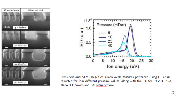
- Ion/Neutral Ratio Insights: Neutral reactive transport is crucial in addressing ARDE issues (see Figure 18). In plasma semiconductor processing, the mean free path between gas phase collisions often exceeds feature size, causing neutral deficiency. Measuring the ion-to-neutral ratio, the Quantum system optimizes this ratio to reduce ARDE. Understanding the ion/neutral ratios hitting the surface is key to understanding the chemical reactions and limiting factors of the etching process.
- Aspect Ratio Understanding: Utilizing capillary plates with different aspect ratios, the Quantum system provides detailed analysis of ion and neutral behavior, helping to mitigate twisting and critical dimension variations.
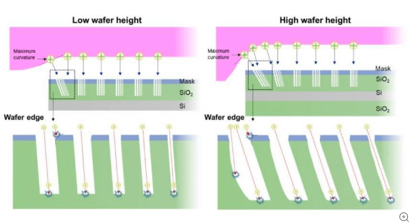
The Langmuir probe is essential for understanding plasma uniformity across the wafer, a key factor in improving etch profiles, especially at the wafer edge. Here’s how it helps:
- Plasma Uniformity Analysis: The Langmuir probe measures electron density and temperature, providing insights into plasma uniformity. This information is critical for adjusting process parameters to achieve consistent etch profiles across the wafer.
- Edge Profile Improvement: By ensuring uniform plasma conditions, the Langmuir probe helps mitigate edge-related etch issues, thereby improving overall wafer yield.
For more details on how plasma uniformity impacts etch processes, see our section on plasma uniformity.
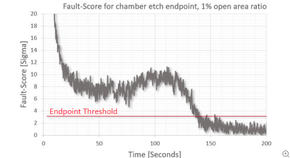
The VI sensors are instrumental in detecting the etch end point, reducing the risk of over-etching or under-etching, and ensuring precise etch profiles. Here’s how they contribute:
- Accurate End Point Detection: VI sensors provide real-time data on plasma impedance and voltage, enabling precise end-point detection in sceanrios where optical end-point systems do not detect end points.
- Reducing Over/Under Etching: By accurately identifying the etch end point, VI sensors help prevent over-etching and under-etching, ensuring the desired etch profile is achieved.
For more information on how end-point detection can optimize your etching process, see our section on end point detection.
Impedans solutions to control etch rates
Impedans offers a range of solutions to control plasma-induced damages. The Langmuir probe offers real time measurement of electron density, electron temperature, and plasma potential. Maintaining optimal density and temperature is essential for controlling etch rates. The Semion RFEA measures the energy distribution of ions reaching the substrate, providing insights into the etching process. By controlling ion energy, users can fine-tune the etch rate. The Octiv VI probes measure critical parameters such as RF voltage, current, phase, and harmonic content. By monitoring these parameters in real-time, users can optimize the power delivery to the plasma, which directly affects the etch rate. On the substrate side, Octiv VI probe can be used to optimize the DC/pulsed DC/ pulsed RF parameters on wafer to optimize the process and control the etch rates.


Plasma-Induced Damage in Plasma Processing
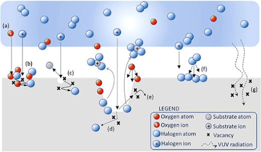
Despite advancements in plasma processing, material degradation, known as plasma-induced damage (PID), remains an issue. PID is typically categorized into three types: physical, charging, and radiation damage.
High-energy ion bombardment causes physical damage to silicon substrates and other surfaces. Energetic ions, accelerated across plasma sheaths, can range from tens to hundreds of eV, leading to lattice displacement, trap generation, interlayer mixing, chemical bond damage, surface state alterations, and implantation.
- Figure 21 illustrates the main mechanisms through which energetic ions cause physical damage. Monitoring the ion energy and flux reaching the wafer during the process is crucial to mitigate this damage.
- Sidewall damage from ions bombardment, while typically minimal, can still be important. Measurement of the ion trajectories enable the modification on process parameters and restrict the ions within the specific angular range to minimize the damage.
- Plasma non uniformity across the wafer can also lead to variation in ion surface interaction and hence the surface properties may change. Ensuring uniform plasma distribution is essential to maintain consistent surface characteristics and reduce the potential for damage. Understanding and controlling these factors are critical for improving plasma processing outcomes and minimizing plasma-induced damage.
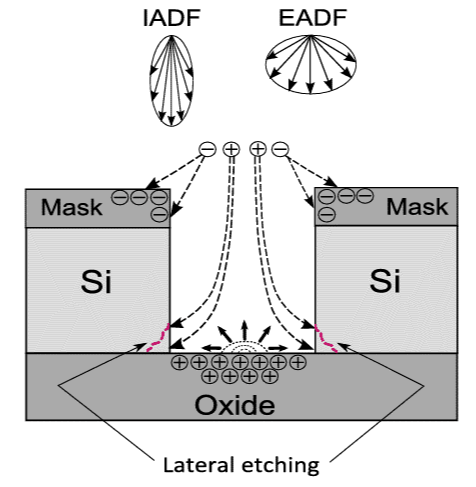
Charging damage happens when insulating surfaces are hit by unequal ion and electron fluxes, causing the surfaces to accumulate charge. This charge creates local electric fields that alter ion trajectories, leading to changes in etching profiles like bowing and notching, especially in high aspect ratio trenches, as shown in Figure 22. In thin dielectrics, charge build-up can result in current flow during discharge, generating traps. In severe cases, this can cause arcing between features, particularly near the end of etching when the dielectric is thin. To mitigate charging damage, controlling density and potential gradients in large-area plasma sources is essential. Techniques like applying pulsed plasma or pulsed bias at the wafer help minimize these issues. Precise control over plasma uniformity, including electron density and plasma potential, is crucial for effective management.
High-energy photon interactions break chemical bonds within materials, leading to degradation.
Impedans solutions to control plasma induced damages
Measuring the ion energy distribution with the Semion RFEA helps fine-tune plasma conditions to achieve desired profiles while minimizing energy imparted to the substrate. Lower energy ions reduce physical sputtering and surface damage. Variations in plasma properties across the wafer can cause non-uniform etching and surface damage. Impedans offers capillary plates for integration with the standard Semion system to measure the angular distribution of ion energies and mitigate sidewall damage. Impedans Langmuir Probe tools provide spatially resolved plasma diagnostics, identifying and correcting non-uniformities in plasma parameters to minimize surface damage. Impedans Alfven arc detector tools detect and help mitigate charging effects by optimizing plasma conditions, protecting the integrity of etched features.
Controlling etch rates in plasma etching processes is crucial for achieving precise and consistent results. Here are several factors and strategies to manage and optimize etch rates, including plasma and RF parameters, as well as wafer and mask materials.
Plasma parameters
Etching rates are directly related to the radical and charged particle flux produced in plasma. The more reactive plasma generated by high RF frequency, high power and high pressure has a faster etch rate.
Ion energy and flux
Ion energies and ion flux are key drivers to control the etch rate. Lower pressures typically result in higher ion energies and can increase etch rates. However, higher pressures result in large ion flux hence an optimized pressure range is advised to get higher etch rates.
Substrate Bias
A higher DC bias on the substrate can enhance ion bombardment, increasing the etch rate. Applying a low frequency bias to the substrate can control the energy of ions hitting the substrate, affecting the etch rate. Substrate biasing provides additional knobs to control the ion energy and hence the etch rates.
Pulsed Plasma
Modulating the plasma power in pulses rather than continuous wave can control the ion energy and density, affecting etch rates.
Impedans solutions to control etch rates
Impedans offers a range of solutions to control plasma-induced damages. The Langmuir probe offers real time measurement of electron density, electron temperature, and plasma potential. Maintaining optimal density and temperature is essential for controlling etch rates. The Semion RFEA measures the energy distribution of ions reaching the substrate, providing insights into the etching process. By controlling ion energy, users can fine-tune the etch rate. The Octiv VI probes measure critical parameters such as RF voltage, current, phase, and harmonic content. By monitoring these parameters in real-time, users can optimize the power delivery to the plasma, which directly affects the etch rate. On the substrate side, Octiv VI probe can be used to optimize the DC/pulsed DC/ pulsed RF parameters on wafer to optimize the process and control the etch rates.
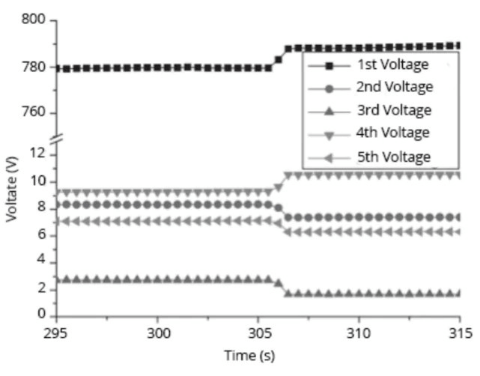
End point detection refers to the process of identifying the precise moment when the etching or cleaning step reaches their completion respectively. Monitoring plasma harmonics is a promising technique to identify the completion of a chamber cleaning process or to indicate when the wafer is etched through. Tracking the change in harmonics indicates the clean and etch end Points.
Detecting when to finish the etching process can be difficult especially for low open area or high aspect ratio etch processes. The RF spectroscopy technique has been found to exhibit superior sensitivity than OES enabling it to be used in complex processing scenarios such as those with less than 1% open area.
Impedans solutions for end point detection:
The RF Spectrometer ‘Moduli’ is an RF detector that monitors the electrical state of a plasma from outside the plasma chamber. It collects RF emissions of harmonics during the process. For example, as etching progresses and the endpoint approaches, changes in plasma composition cause characteristic shifts in RF emissions, which are detected to determine the endpoint. The RF spectrometer shows superior sensitivity, even in complex scenarios with less than 1% open area. Sensitivity channels vary with the plasma recipe and processing tool, monitoring voltage, current, and the phases between them and between harmonic and fundamental RF waves. By comparing live data to a baseline collected when the layer was not etched, a clear endpoint signal is defined.