Plasma uniformity
Plasma uniformity is critical in semiconductor manufacturing, particularly during processes like etching, deposition, and surface treatments. Plasma uniformity directly influences both the efficiency of semiconductor processes and the yield of viable products. By ensuring uniform plasma conditions, manufacturers can optimize their processes, reduce defects, and improve overall productivity.
By ensuring uniform plasma conditions, manufacturers can optimize their processes by obtaining consistent etching and deposition rates. Variability can lead to longer processing times or multiple runs to achieve desired uniformity, decreasing overall efficiency. Issues related to plasma non-uniformity often require troubleshooting and adjustments. By maintaining uniformity, manufacturers can minimize downtime and streamline operations.
Wafer yield is a critical metric for semiconductor manufacturing. It is represented by the functionality and reliability of integrated circuits produced on the wafer surfaces. During the manufacturing of integrated circuits yield loss is caused for example by defects, faults, process variations, and design. Plasma uniformity ensures lesser yield loss in multiple ways as given below.
Reduced edge die loss
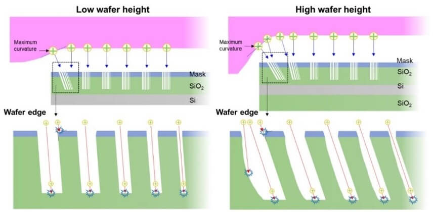
Since the particle flux reaching the edge of wafer is not same as reaching to its center, the process of etching and deposition are less controlled on t e periphery of the circular wafer, manufacturing accuracy is poor, leading to edge die losses. It is seen that edge effects are more prominent on small size wafers. Increased uniformity towards end will lead to lo er die loss on the periphery.

Figure 1 Plasma non uniformity near the wafer edges and its effect on critical dimension (Reference Controlling Uniformity At The Edge (semiengineering.com)
Defect Reduction
Non-uniform plasma can cause variations in etch depth and deposition thickness, leading to defects such as incomplete etching or film delamination. These defects reduce the yield of functional devices. Uniformity of plasma help to reduce these defects.
Lower Scrap Rates
The spatial nonuniformity of plasma leads to a local imbalance between electron and ion currents from the plasma. The imbalance of local particle currents from the plasma leads to gate charging and subsequent gate oxide degradation. The damage mainly occurs at the end point and during the over-etch. With improved plasma uniformity, the likelihood of havi g to scrap wafers due to defects decreases, thus improving yield.
Tighter Process Control
Uniform plasma allows for tighter process tolerances, enabling manufacturers to produce more devices within specification, further enhancing yield.
Key factors contributing to plasma nonuniformity
Inhomogeneous Gas Distribution:
Variability in gas flow can lead to uneven plasma density.
Electrode Design:
Non-optimized electrode geometry can cause uneven electric fields, affecting plasma uniformity.
Wafer Loading Variations:
Different wafer sizes or loading patterns can disrupt plasma consistency across the substrate.
Power Distribution:
Uneven power delivery to the plasma can create hotspots, leading to non-uniform reactions.
Chamber Contamination:
Residues and particles in the chamber can lead to localized plasma variations.
Temperature Gradients::
Variations in temperature across the substrate can affect plasma behavior and material interactions.
Impedans solutions for monitoring plasma uniformity:
Addressing plasma uniformity issues is essential for achieving high-quality semiconductor devices. By utilizing advanced monitoring techniques, manufacturers can enhance plasma uniformity and improve overall process reliability and yield.


Impedans solutions for monitoring plasma uniformity:
Addressing plasma uniformity issues is essential for achieving high-quality semiconductor devices. By utilizing advanced monitoring techniques, manufacturers can enhance plasma uniformity and improve overall process reliability and yield.
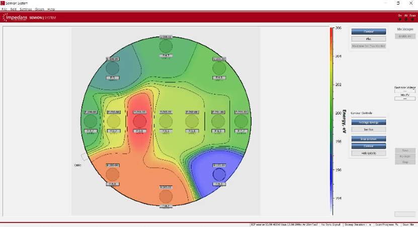
Semion RFEA System for Ion Energy and Flux control
The Semion RFEA system measures key process parameters such as the ion flux and ion energy distribution hitting a surface in real-time using an imitation substrate (holder plate) with integrated sensors. The Semion Multi Sensor system can have up to 13 sensing elements distributed around the imitation substrate, which is primarily used to investigate the uniformity of ion energy and ion flux at the substrate. Precise control over ion flux distribution helps in reducing variability and achieving consistent profiles across the wafer.
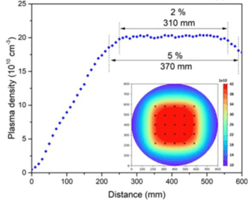
Langmuir Probe for plasma measurements
The Langmuir probe is essential for understanding plasma uniformity across the wafer, a key factor in improving etch profiles, especially at the wafer edge. Here’s how it helps:
Plasma Uniformity Analysis: The Langmuir probe measures electron density and temperature, providing insights into plasma uniformity. This information is critical for adjusting process parameters to achieve consistent etch profiles across the wafer.
Edge Profile Improvement: By ensuring uniform plasma conditions, the Langmuir probe helps mitigate edge-related etch issues, thereby improving overall wafer yield.